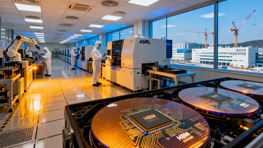

When a single chipmaker commits over $70 billion to one bet, it tells you something about where the industry thinks the center of gravity is shifting. SK Hynix is not hedging. It is going all in on the conviction that AI’s appetite for memory will not just grow but fundamentally reshape how chips are built, packaged, and delivered.
The numbers alone are staggering. More than 100 trillion won earmarked for new fabrication and advanced packaging facilities, with the crown jewel being the M15X fab in Cheongju. That facility is on track to become the world’s first production base dedicated entirely to HBM4, the next generation of high bandwidth memory that AI accelerators from Nvidia and others are expected to demand in enormous quantities starting late 2025. A separate 19 trillion won packaging plant rounds out the strategy, targeting what has quietly become one of the most stubborn constraints in the semiconductor supply chain.
But the investment thesis here goes deeper than just building more capacity.
For years, memory was treated as a commodity business. Cycles of oversupply and price crashes defined the DRAM and NAND markets. Companies built fabs, flooded the market, watched margins collapse, and then pulled back. SK Hynix, Samsung, and Micron danced this painful waltz for decades. What changed is that HBM broke the pattern. High bandwidth memory is not a commodity. It requires sophisticated 3D stacking, advanced packaging techniques like thermocompression bonding, and extremely tight integration with logic chips. The margins are dramatically better, but the manufacturing complexity is a genuine barrier to entry.
This is precisely why SK Hynix is spending so aggressively on packaging specifically. The industry has talked about packaging bottlenecks for two years now, and for good reason. You can fabricate all the HBM dies you want, but if you cannot stack them, bond them, and test them at scale, those dies sit in inventory. The dedicated 19 trillion won packaging facility is an acknowledgment that the real constraint in AI memory is not wafer production. It is everything that happens after.
Consider the timeline. HBM4 is expected to double the bandwidth of HBM3E while pushing stack heights to 16 layers. Each generation has introduced new yield challenges. HBM3E already pushed thermocompression bonding to its limits, and industry chatter suggests that hybrid bonding may become necessary for HBM4 at full stack heights. SK Hynix choosing to build a dedicated fab rather than retrofit existing lines signals confidence that HBM4 volumes will justify purpose built infrastructure. That is not a trivial assumption. It implies that the company’s order book, likely anchored by Nvidia’s Rubin platform, provides enough visibility to underwrite this kind of capital expenditure.
Still, there are real risks embedded in this strategy. The AI accelerator market remains concentrated among a handful of buyers. If training workloads plateau or shift toward more memory efficient architectures, demand projections could soften faster than new capacity can be absorbed. SK Hynix experienced exactly this kind of whiplash in 2019 when a datacenter spending pause left it sitting on excess DRAM inventory. The difference now is that HBM fabs are far more expensive and far less flexible than conventional DRAM lines. You cannot easily repurpose an HBM4 production base for standard server memory.
There is also the competitive dimension. Samsung has been scrambling to close the gap in HBM3E yields and reportedly accelerating its own HBM4 development timeline. Micron, meanwhile, has carved out a meaningful position with its 12 layer HBM3E and is investing in its own advanced packaging capabilities. The window of technical leadership that SK Hynix currently enjoys is real but not permanent.
What makes this moment particularly interesting is the packaging plant decision. Historically, OSAT companies like ASE and Amkor handled much of the advanced packaging work for the industry. By bringing high volume HBM packaging entirely in house, SK Hynix is vertically integrating in a way that reduces its dependence on external partners and gives it tighter control over yield and throughput. Samsung has done something similar with its own packaging lines. The implication for the broader ecosystem is clear: as AI memory becomes the highest margin segment in semiconductors, the major players are pulling critical manufacturing steps inside their own walls.
For the broader AI industry, SK Hynix’s investment validates a fundamental assumption. The models are getting bigger. The inference workloads are scaling. And the memory wall, that persistent gap between what processors can compute and what memory can feed them, is only becoming more acute. HBM4 is not a solution to that problem so much as the next escalation in an ongoing arms race between compute and memory bandwidth.
The Q4 2025 operational target for M15X also matters for a more prosaic reason. It aligns almost perfectly with when Nvidia is expected to ramp its next generation platform. Semiconductor investments of this scale do not happen in isolation. They are coordinated, sometimes years in advance, between memory suppliers and their largest customers. The timing here strongly suggests that SK Hynix has secured commitments that justify moving this fast.
Whether this bet pays off will depend on whether AI spending sustains its current trajectory through the back half of the decade. The capital is committed. The fabs are being built. Now the question is whether the world needs as much AI memory as SK Hynix is preparing to make.
When a single chipmaker commits more than 100 trillion won to new fabrication plants and packaging facilities in the span of a few years, it tells you something about where the semiconductor industry believes the money will be made for the next decade. SK Hynix is not hedging its bets. The company is going all in on artificial intelligence memory, and the scale of that commitment deserves closer examination than the headline numbers alone can provide.
The investment is not happening in a vacuum. AI accelerators from Nvidia, AMD and a growing list of custom silicon designers are all memory hungry in ways that previous generations of chips simply were not. High bandwidth memory has become the critical bottleneck. You can design the most powerful GPU architecture in the world, but if you cannot feed it data fast enough, performance suffers. SK Hynix recognized this dynamic earlier than most, and its position as Nvidia’s primary HBM supplier gave it both the revenue certainty and the strategic motivation to spend aggressively.
At the center of the near term plan sits the M15X fab in Cheongju, which SK Hynix has positioned as the world’s first production base dedicated entirely to HBM4. The facility received more than 20 trillion won in investment and began operations ahead of schedule in Q4 2025. Mass production of HBM4 launched in February 2026. Monthly wafer capacity started at roughly 10,000 wafers and is expected to reach between 55,000 and 60,000 by the end of 2026. That ramp rate is ambitious. It also reflects genuine confidence in demand visibility, because nobody builds out capacity that fast unless customer commitments are already locked in.
Then there is Yongin. The first phase of SK Hynix’s semiconductor cluster there has secured 31 trillion won, with operational start pulled forward to February 2027. The corporate roadmap calls for a doubling of total memory wafer capacity within five years, and the priority is clearly on HBM and advanced node DRAM rather than commodity products. This is a deliberate strategic choice. Commodity DRAM remains a cyclical business with thin margins during downturns. AI memory, at least for now, commands pricing power that commodity memory has not enjoyed in years.
But fabricating memory wafers is only half the equation. Packaging those chips into the complex 3D stacked configurations that HBM requires has emerged as its own constraint. SK Hynix has allocated approximately 19 trillion won toward a dedicated AI memory packaging plant. The P&T7 facility in Cheongju’s Techno Polis complex will span roughly 231,000 square meters, which would make it the largest site of its kind globally. Construction starts in April 2026, with the main building targeted for completion by late 2027 and volume operations coming toward the end of the decade. The timing is deliberate. It aligns with the expected deployment windows for HBM4E, HBM5 and HBM5E, each generation demanding more sophisticated packaging than the last.
This packaging investment matters more than it might first appear. Across the industry, advanced packaging capacity has become the chokepoint that limits how many AI accelerators can actually ship. TSMC faces similar constraints with its CoWoS packaging for Nvidia’s GPUs. By building dedicated packaging infrastructure at this scale, SK Hynix is trying to ensure that its own memory production is not bottlenecked by someone else’s packaging capacity. Vertical integration of this kind gives the company more control over its supply chain and, critically, more leverage with customers.
Zoom out further and the numbers get even larger. Within SK Group’s broader roadmap, total commitments reach approximately 1,100 trillion won to scale HBM and next generation DRAM production over multiple years. That figure includes contributions from across the group, not just SK Hynix alone, but it signals an institutional conviction that AI memory will be a defining growth market for the foreseeable future. This conviction is shared at the national level, where SK Hynix’s plans form part of a $2.1 trillion joint initiative with Samsung Electronics aimed at spreading AI-driven economic benefits across the country.
The economic backdrop supports the bet. A tightening global memory chip shortage has pushed HBM prices higher and improved margins significantly. SK Hynix’s HBM revenue has grown at rates that would have seemed implausible just three years ago. Additionally, this investment aligns with the trend of circular financing in the semiconductor industry, where suppliers bolster customer capabilities to drive their own sales.
Still, there are risks worth noting. Memory markets are notoriously cyclical. Every previous generation of aggressive capacity expansion eventually ran into a demand correction. The question is whether AI workloads represent a structural shift large enough to smooth out those cycles, or whether the industry is once again building toward oversupply.
For now, the evidence favors SK Hynix’s thesis. Every major cloud provider is expanding AI infrastructure. Training runs keep getting larger. Inference workloads are scaling rapidly as AI models move into production. All of this requires more memory bandwidth, not less.
And SK Hynix, by moving first and moving fast, has positioned itself to capture a disproportionate share of that demand. Whether the company can sustain its execution at this pace over a five year horizon will determine whether this turns out to be one of the great capital allocation decisions in semiconductor history, or a cautionary tale about building too much, too fast.