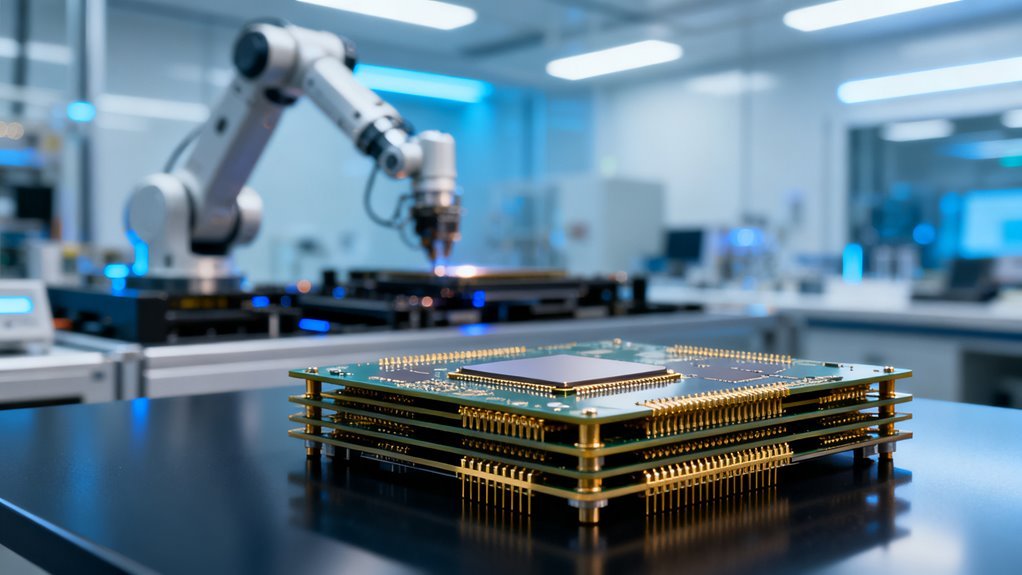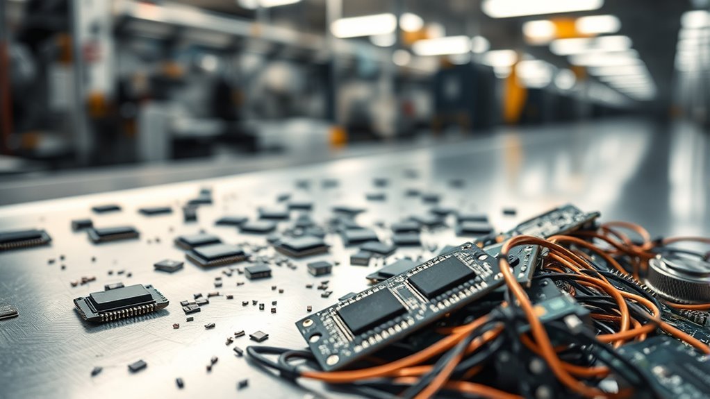

Advanced AI chips rest on a tightly engineered stack of materials, from ultra‑pure silicon substrates and precisely controlled dopants to wide‑bandgap compound semiconductors, high‑performance interconnect metals, and low‑k dielectrics tailored for 3D integration. Ultra‑pure silicon wafers provide the foundational substrate for dense AI logic and memory, hosting billions of transistors per die while maintaining low defect densities and consistent electrical behavior. Controlled introduction of dopants such as boron, phosphorus, and arsenic tunes silicon conductivity, forming p–n junctions and high‑density CMOS structures that underpin AI accelerators and supporting circuitry. This engineering precision is crucial as memory price inflation impacts the overall production costs of AI chips.
AI performance starts with ultra‑pure silicon and dopants, building dense, reliable CMOS foundations for accelerators
Choice of dopant species influences not only device performance but also reliability under extreme operating conditions common in AI data centers. Arsenic‑doped regions offer greater thermal stability than phosphorus‑doped regions at high voltage and high temperature, supporting transistors that must switch rapidly while withstanding substantial power density.
Beyond silicon, critical elements such as gallium and germanium enable high‑performance computing and high‑speed data transmission, yet their production remains geographically concentrated, exposing AI infrastructure to supply and geopolitical risks. Germanium’s higher electron mobility than silicon enhances high‑speed I/O and fiber‑optic links that connect accelerators across racks, and these communication functions now account for a significant fraction of global germanium demand.
Power delivery for advanced AI servers increasingly depends on wide‑bandgap semiconductors such as silicon carbide and gallium nitride, which offer higher breakdown voltage, faster switching, and lower conduction losses than conventional silicon devices. SiC MOSFETs enable high‑voltage, high‑temperature stages in multi‑kilowatt server power supplies, including three‑phase interleaved power‑factor‑correction front ends for racks approaching 12 kilowatts of continuous load. Across the semiconductor landscape, wide‑bandgap semiconductors are emerging as a central battleground where AI companies and power‑device manufacturers compete to deliver higher‑efficiency, lower‑cost computing infrastructure.
GaN power ICs support high‑frequency LLC converter stages with superior power density, shrinking the size of power modules and freeing valuable volume for additional accelerator cards within constrained rack footprints. As data centers migrate from legacy low‑voltage distribution toward approximately 800‑volt direct‑current architectures, these wide‑bandgap devices become essential for achieving acceptable efficiency, thermal margins, and system cost.
Compound semiconductors such as gallium arsenide further enhance the surrounding ecosystem, enabling high‑speed radio‑frequency links, optical transceivers, and emerging quantum‑related functions that orchestrate data flow between AI chips and memory tiers.
Inside each AI processor, performance increasingly hinges on advanced interconnect metals and engineered liners that carry signals across shrinking geometries without excessive resistance or reliability loss. Copper has become the dominant interconnect material, displacing aluminum through its lower resistivity and enabling dense routing with reduced voltage drop across large AI dies.
Tantalum diffusion barriers prevent copper migration into surrounding dielectrics and silicon, preserving device integrity, while binary ruthenium–cobalt liners allow liner thickness near two nanometers and reduce interconnect resistance at leading‑edge nodes. Tungsten, tungsten silicides, and titanium silicide provide low‑resistivity, thermally stable contacts and via‑fill structures whose high melting point and low thermal expansion support long‑term reliability in high‑power AI processors.
Low‑k dielectrics and 3D integration minimize signal delay and sustain scaling efficiency.