The memory industry just telegraphed where AI hardware is heading for the rest of the decade, and the implications run deeper than spec sheet improvements.
Samsung’s newly unveiled roadmap through 2030 centers on something called zHBM, an architecture that fundamentally rethinks how memory and compute relate to each other. Rather than connecting memory chips to AI accelerators through traditional packaging, zHBM bonds high bandwidth memory directly onto the accelerator itself. The claimed numbers are staggering: 8x the performance of HBM5, 10x the memory density, and meaningful gains in energy efficiency. If even half of that materializes, it would represent the kind of architectural leap the industry has been chasing since the memory wall became AI’s most stubborn constraint.
But let’s slow down and put this in context.
For years, the AI conversation has fixated on GPU compute power. NVIDIA’s stock price became a proxy for AI progress. What received far less attention was the growing mismatch between how fast processors could crunch numbers and how quickly memory could feed them data. That gap, the memory wall, has quietly become the binding constraint on model training and inference at scale. Every major AI lab has felt it. Larger models demand more parameters held in memory, faster access patterns, and lower latency. The processors are hungry, and the memory subsystem can’t keep the plate full.
Samsung’s near term moves reflect this urgency. HBM4 is entering mass production targeting NVIDIA and AMD platforms, which means the next generation of data center GPUs will ship with substantially more memory bandwidth than what’s available today. Meanwhile, Samsung’s V10 NAND pushes past 400 layers, continuing the vertical scaling trend that has defined flash storage for the better part of a decade.
These incremental advances matter on their own. Yet zHBM is the one worth watching closely.
The idea of tightly coupling memory and compute isn’t new. It echoes concepts from processing in memory research that academic groups explored in the 2010s, and it shares DNA with what companies like SK Hynix and Micron have been exploring through advanced packaging. What makes Samsung’s announcement significant is the specificity of the performance targets and the fact that they’ve planted a flag on a public timeline. Roadmaps from memory manufacturers carry weight because these companies operate on multi year fabrication cycles. Announcing zHBM for 2030 means Samsung is already allocating R&D resources, designing process nodes, and likely engaging early customers.
The strategic calculus here is also worth examining. Samsung has been losing ground to SK Hynix in the HBM market. SK Hynix secured early wins with HBM3E supply to NVIDIA and built a production lead that Samsung has been scrambling to close. Launching an aggressive long term roadmap serves a dual purpose: it reassures customers that Samsung has a credible path forward, and it forces competitors to respond with their own timelines.
For AI companies and cloud providers planning infrastructure investments, the practical question is whether zHBM’s direct bonding approach will require entirely new accelerator designs or whether it can integrate with existing architectural paradigms. If it demands co design from the ground up, then Samsung is essentially asking the industry to commit to its memory ecosystem years in advance. That’s a bold play, and one that could either cement Samsung’s position or create openings for rivals if the technology hits delays.
One thing is already clear. The center of gravity in AI hardware is shifting. Compute alone won’t define the next era. Whoever solves the memory problem most effectively will shape which models are trainable, which applications become practical, and ultimately how fast the entire field can move. Samsung is betting billions that it will be the one holding that key.
The memory wall has been the quiet bottleneck behind every headline about AI scaling. While the industry fixates on GPU counts and model parameter records, the real constraint sits one layer deeper: how fast you can feed data to silicon that’s hungry for it. Samsung just laid out its answer at FMS 2026, and it’s ambitious enough to reshape how we think about where compute ends and memory begins.
The memory wall, not the GPU, is the real bottleneck holding back AI — and Samsung is attacking it at the physics level.
The roadmap isn’t a single product announcement. It’s a full stack vision spanning DRAM, HBM, CXL attached memory, and storage class innovations built on advanced NAND. The target is roughly 10x higher token throughput by decade’s end. That number matters because it tracks directly to inference cost, training speed, and ultimately how many organizations can afford to run frontier models at scale.
zHBM: Fusing Memory and Compute Into a Single Vertical Stack
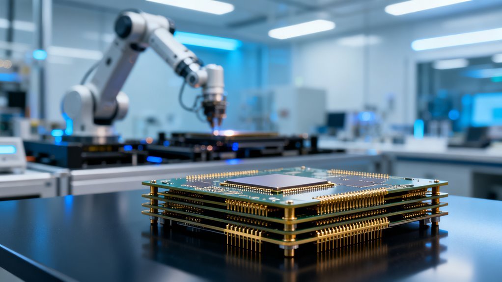
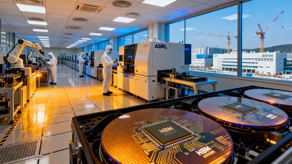
The most provocative element here is zHBM, a concept architecture that would bond high bandwidth memory directly onto AI accelerator dies using wafer level integration. Samsung is claiming targets of approximately 8x the performance of HBM5, more than 10x the memory density, around 3x better energy efficiency, and at least 50% lower thermal resistance. Those are not incremental improvements. If realized, they represent a fundamental change in how AI chips are constructed.
What makes zHBM significant isn’t just the numbers. It’s the architectural philosophy. For years, memory and compute have been manufactured separately and connected through interposers or package substrates that introduce latency, burn power, and generate heat. Samsung is signaling that the next competitive frontier involves collapsing that gap entirely. This shift toward grid stability is essential for ensuring that the increased power demands of AI data centers do not destabilize the electric grid.
Vertically fused compute and memory modules would shrink interconnect distances to near zero, which is exactly the kind of physical optimization that can’t be replicated through software tricks or compiler improvements. This long-term concept is designed specifically to address the demands of future AI infrastructure rather than serve as an immediate product release.
But concept architectures are easy to announce. The execution timeline remains unclear, and wafer bonding at this density brings yield challenges that Samsung hasn’t publicly addressed. Still, the direction is telling. It suggests Samsung sees the future of AI hardware as an integration problem, not merely a bandwidth problem.
HBM4 and HBM4E: The Near Term Battle for AI Platform Wins
Closer to the present, Samsung is executing across two HBM generations that will define competitive positioning over the next 18 to 24 months. HBM4 has entered mass production targeting the NVIDIA Vera Rubin platform at 11.7Gbps per pin, with a path to 13Gbps. HBM4E pushes further to 16Gbps per pin and 4.0TB/s bandwidth per stack.
The platform wins tell an important story. Samsung has secured primary HBM4 supply for AMD’s Instinct MI455X GPU alongside its NVIDIA allocation, and the company is offering custom HBM variants tuned to specific accelerator requirements. This customization angle deserves attention.
As AI chip architectures diverge across vendors, a memory supplier that can tailor its products to individual accelerator thermal profiles and signaling requirements gains a meaningful structural advantage over competitors offering more standardized parts.
For context, SK hynix has dominated HBM supply relationships over the past two years, particularly with NVIDIA. Samsung’s dual platform wins with both NVIDIA and AMD suggest the competitive gap may be narrowing. Whether that holds depends on yield performance and actual power efficiency in deployed systems, metrics that don’t show up in press releases.
V10 NAND and the Storage Class Memory Play
On the storage side, Samsung introduced V10 BV NAND with more than 400 layers built using wafer bonding technology. The density improvement over V9 sits around 58%, accompanied by faster read, write, and I/O performance. This is evolutionary progress, but the cumulative effect of layer count scaling is starting to change what NAND based storage can do for AI workloads.
More interesting is zNAND O, an architecture that borrows 3D NAND advances to deliver storage class memory behavior optimized for AI. This sits in the gap between DRAM and traditional SSDs, a space where Intel’s Optane once operated before its discontinuation.
Samsung is essentially rebuilding that tier of the memory hierarchy using its own technology stack, which gives it vertical integration advantages Intel never fully achieved with Optane. The strategic logic is straightforward. Large language models and multimodal systems increasingly require capacity that exceeds what HBM alone can provide economically.
A full stack approach, where HBM handles the hottest data, DRAM covers working sets, and zNAND manages larger context windows or model weight staging, lets Samsung sell into every layer of the AI memory hierarchy rather than competing on a single product line.
What This Actually Means for AI Infrastructure
Samsung’s roadmap is structured around four pillars: bandwidth, capacity, thermal management, and security. The first three are engineering problems with clear technical paths. Security is the wildcard.
As AI infrastructure moves toward confidential computing and multi-tenant deployment, memory level security features could become a differentiator that influences purchasing decisions at the hyperscaler level.
The broader implication is that memory technology is becoming a first order constraint on AI progress in ways that weren’t true even three years ago. Model sizes continue growing. Inference demand is scaling faster than training demand.
And the economics of AI deployment increasingly hinge on energy efficiency per token, a metric where memory power consumption plays an outsized role. Samsung is betting that whoever solves the physical integration of memory and compute, not just the bandwidth spec sheet, will own the next decade of AI infrastructure. That’s a bold thesis. It’s also probably correct.